How To Implement An AND Gate Using Logic Chips
Today I’m going to show you how to physically implement one of the most fundamental logic gates: the AND gate.
Now anyone who has taken a computer systems class has likely seen this symbol.

I’m not going to spend time explaining the boolean logic of the AND gate as your professor likely already covered it many times. However, one thing that your professor probably forgot to mention is that logic gate symbols are just a mere abstraction of the actual physical circuitry that gets implemented.

There are actually many physical implementations of circuit logic that can be used to build an AND gate. But we are going to be looking at one implementation in particular called Transistor-Transistor Logic (TTL). We are not going to be actually designing the electrical circuits in the diagram. That level of detail belongs to the domain of electrical engineers. It’s better to use what's called an integrated circuit (IC) that packages all of those transistors, resistors, and diodes onto a well tested, small chip. So let’s find a chip…
The 7400 series is a family of logic chips created by Texas Instruments that use TTL. Introduced in 1964, they are old but incredibly reliable and widely used for small/medium scale integrations.

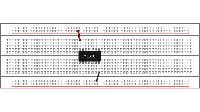
We are going to be using the 74LS08. This is a chip that has 4 AND gates that each take 2 inputs but we will only be using 1 gate. When working with physical chips it is good practice to first pull up the datasheet.
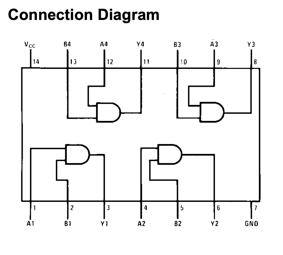
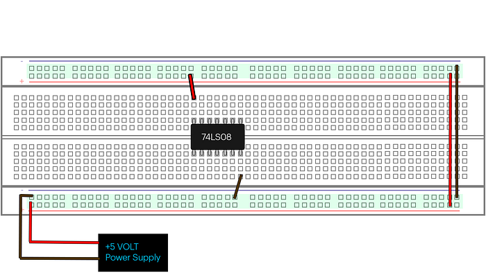
On the datasheet, you will find a connection diagram with AND gate symbols. We’re going to place our chip on a breadboard. First, we’ll start by connnecting our chip to power (pin 14) and to ground (pin 7).
But how much power does our chip need? On the datasheet, under recommended operating conditions find VCC.

It says that we need a minium of 4.75 volts and we shouldn’t exceed a maxium of 5.25 volts. So we’re going to need connect 5 volts of power to the power rail.
Next we need to connect our 2 inputs from the datasheet, A3 (pin 9) and B3 (pin 10). Now we know that an AND gate needs at least 2 high inputs to get a high output.
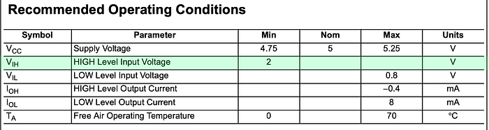
On the data sheet find VIH this stands for worst case high input and it says we need a min of 2 volts. What this means is that we can decrease our input voltages (A3, B3) all the way down to 2 volts and it will still remain a high input to the chip.
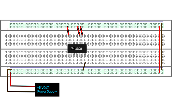
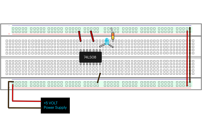
With that we can connect our inputs directly to 5 volts and the chip will accept it as a high input. And boom! We have succesfully set up our AND gate. The circuits contained inside the chip will handle the ANDing logic and produce an output at Y1 (pin 8). Sadly we can’t actually see any visual output occuring right now so lets hook up an LED.

Make sure the anode of the LED lines up with the row Y1(pin 3). Then put a 220k resistor to ground and line it up with the cathode. If everything is hooked up correctly then you should see the LED light up. Let’s see our gate work in action. Remove the connection between A3 and power; you will see the LED turn off. Viola we confirmed our AND gate is working!
Congratulations, you have succesfully implemented an AND gate using a singular logic chip. Now we only implemented 1 logic gate but getting a strong understanding of TTL logic chips will enable you to understand other logic families and technolgies with greater ease. In a future tutorial I will teach you how to build a more complex circuit with more types of logic chips. In addition to covering important topics like power dissipation and propagation delay.